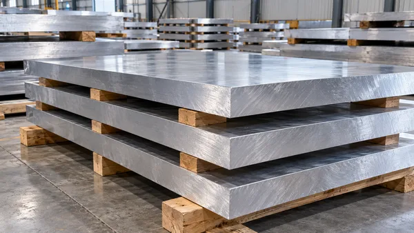
Pure aluminium (5N – 5N5)
Used for electrodes, reflective films, backside metal and as a base for alloy films. Highest conductivity of the aluminium options, but more prone to hillocks and electromigration than alloyed films.



Sputtering targets are the solid metal plates that physical vapour deposition (PVD) tools bombard with ions to deposit thin films on wafers. Each film in a device, from interconnect and barrier layers to contacts and backside metal, calls for a particular target material, purity and grain structure. This guide explains which materials are used where and what to specify. Metline supplies aluminium and aluminium-alloy targets (Al, AlCu, AlSi, AlSiCu) and aluminium backing plates; the other metals are described for comparison.
In magnetron sputtering, argon ions are accelerated into the target surface inside a vacuum chamber. Each impact knocks atoms off the target, and those atoms travel to the wafer and condense into a film a few nanometres to a few micrometres thick. The target is consumed slowly over thousands of wafers, and everything in it, including impurities, inclusions and grain structure, is transferred into or affects the film.
Three target properties therefore drive film quality. Purity matters because trace impurities such as alkali metals, uranium and thorium, or excess iron, degrade device reliability; semiconductor targets are commonly 5N (99.999 %) or better. Microstructure matters because grain size and crystallographic texture control the sputter rate and the angular distribution of atoms, and so the film thickness uniformity across the wafer and over the life of the target. Soundness and bonding matter because voids, inclusions or a poorly bonded backing plate cause arcing, particles and overheating.
Targets are made to fit specific PVD tools. Planar circular targets for 200 mm and 300 mm wafer chambers are the most common format, with the target either machined as one piece (monolithic) or bonded to a backing plate that carries the cooling interface and mounting features.
| Film function | Typical target materials | What the film must do |
|---|---|---|
| Interconnect and wiring (aluminium metallisation) | Al-0.5 % Cu, Al-1 % Si, Al-1 % Si-0.5 % Cu, pure Al | Low resistivity, resistance to electromigration and hillocks, good etch behaviour |
| Interconnect seed (copper damascene) | Cu, CuMn (comparison) | Continuous seed for copper electroplating; Mn alloy forms a self-barrier |
| Barrier and liner | Ti / TiN with Al; Ta / TaN with Cu (comparison) | Stop diffusion between metal and silicon or dielectric |
| Adhesion layer | Ti, TiW (comparison) | Bond the metal stack to oxide or nitride |
| Contacts and silicides | W, Co, Ni, NiPt (comparison) | Low contact resistance and thermal stability |
| Bond pads and top metal | Al-Cu, Al-Si-Cu | Wire-bondable surface, thick low-resistance top metal for power routing |
| Power device front and back metal | Al, AlSi, AlSiCu front; Ti/Ni/Ag back (comparison) | Carry high current, accept heavy aluminium wire bonds, solderable back side |
| MEMS, sensors and displays | Al, AlSi, AlNd and other Al alloys | Conductive and reflective films, electrodes and mirrors |
Although copper replaced aluminium for the lower wiring levels in advanced logic, aluminium alloys remain in very wide use: in the top metal and bond pads of most chips, in analog, mixed-signal and power devices, in MEMS and image sensors, and in many mature-node fabs that make the majority of chips by volume. Aluminium is also the standard front-side metal of IGBTs, MOSFETs and SiC devices, because it accepts heavy aluminium wire bonds.
Used for electrodes, reflective films, backside metal and as a base for alloy films. Highest conductivity of the aluminium options, but more prone to hillocks and electromigration than alloyed films.
Copper segregates to grain boundaries and greatly slows electromigration, which is why Al-Cu became the standard interconnect alloy. Copper contents from about 0.5 % to 1 % are typical; the exact value is set by the fab.
Silicon in the film prevents the aluminium from dissolving silicon from shallow junctions ("junction spiking"). Common in power devices and older contact schemes.
Combines junction protection and electromigration resistance. Widely used for power semiconductor front metal and bond pads.
Alloys such as Al-Nd and Al-Ti are used in displays and specialised devices for hillock resistance and thermal stability.
Aluminium alloy backing plates (for example 6061) are light, machine well and match the thermal expansion of aluminium targets, reducing bond stress.
| Parameter | What to specify for aluminium targets |
|---|---|
| Purity | Base aluminium purity (for example 5N or 5N5) and maximum limits on critical impurities such as Fe, Si (where not an alloying element), Na, K, U and Th |
| Alloy composition | Nominal Cu and/or Si content and tolerance; uniformity across the target |
| Grain size | Average and maximum grain size, typically fine and uniform through the thickness |
| Texture | Preferred crystallographic orientation if your process requires it |
| Inclusions and voids | Ultrasonic inspection of the target body; acceptance criteria |
| Dimensions | Diameter, thickness, sputter-face profile, mounting holes, O-ring grooves; drawing or tool reference |
| Format | Monolithic, or bonded to backing plate with bond method and bond coverage |
| Surface and cleanliness | Surface roughness, cleaning and vacuum packaging |
More product detail, including standard alloys and sizes, is on our aluminium sputtering targets page, and the base metal grades are explained in the high-purity aluminium guide.
| Material (comparison) | Main use | Notes for engineers |
|---|---|---|
| Copper, CuMn | Seed layers for copper damascene interconnects | Ultra-high purity (6N class) and tightly controlled grain; CuMn forms a self-forming barrier |
| Titanium | Adhesion and barrier (Ti/TiN), especially under aluminium | Often reactively sputtered in nitrogen to form TiN |
| Tantalum | Barrier and liner (Ta/TaN) under copper | Grain size and texture strongly affect film uniformity |
| Tungsten, WTi, WSi | Contacts, gate and barrier layers, UBM | Very hard; usually powder-metallurgy targets |
| Cobalt | Contacts, liners and silicides at advanced nodes | Magnetic; target microstructure is designed for magnetron pass-through flux |
| Nickel, NiPt | Silicide formation, backside and UBM metal | Also magnetic; thin targets used for magnetron efficiency |
Metline does not supply these materials. They are shown so that aluminium film choices can be seen in the context of the whole metal stack.
Target and mounting flange machined from one piece of aluminium alloy. No bond to fail and simple recycling; common for aluminium on many 200 mm and 300 mm tools.
A target plate joined to a separate backing plate. Lets the backing plate be a stronger or more conductive alloy and reused after refurbishment.
Solid-state bond under heat and pressure, giving high strength and thermal conductivity; suits high-power sputtering.
Indium or other low-melting solder; simple and low stress but limited by solder melting point at high power.
Friction stir welding, electron-beam welding and HIP bonding are used for some material pairs and large targets.
Ultrasonic C-scan maps the bond area to find unbonded regions or voids before shipment.
| Symptom in the film or chamber | Likely target-related cause | What to specify or check |
|---|---|---|
| Arcing and splashing | Oxide inclusions, voids or surface contamination in the target | Ultrasonic inspection of the target body; clean, vacuum-packed delivery; proper burn-in |
| Particles on wafers | Inclusions, nodules, flaking from poorly finished edges or a weak bond | Inclusion limits, edge finish, C-scan bond coverage |
| Thickness non-uniformity that drifts with target life | Coarse or uneven grain and texture through the thickness | Grain size and texture limits through the full thickness |
| Sheet resistance or electromigration out of specification | Alloy content off target or segregated | Composition tolerance and uniformity across the plate |
| Overheating or debonding | Incomplete bond to the backing plate, or warped plate | Bond method suited to sputter power; flatness and bond inspection |
Most of these issues are cheaper to prevent at the specification stage than to diagnose in the fab. Ask for the inspection reports with each target, keep a record of target lot numbers against chamber performance, and include the first-wafer burn-in time in your acceptance plan.
Supplying the existing target drawing or a used target for reference is the fastest way to confirm dimensions and mounting features. For a new film, the process engineer's requirements for sheet resistance, uniformity and particle performance help us suggest the alloy and purity.
Al-0.5 % Cu is the usual choice for aluminium interconnects and bond pads because copper strongly improves electromigration resistance. Al-1 % Si-0.5 % Cu is preferred where the film contacts shallow silicon junctions, as in many power devices.
Aluminium dissolves silicon at elevated temperatures and can spike through shallow junctions. Adding about 1 % silicon saturates the film so it does not take silicon from the substrate.
Typically 5N (99.999 %) or 5N5 for the base aluminium, with additional limits on elements such as alkali metals, uranium and thorium. The exact requirement is set by the fab's film specification.
Both are used. Monolithic aluminium targets are common because the alloy itself is strong enough to form the flange; bonded targets on aluminium or copper-alloy backing plates are used where tool design, power or cost calls for them.
Yes. Fine, uniform grains and a controlled texture give a steadier sputter rate, better film uniformity and fewer particles over the life of the target.
No. Metline supplies aluminium and aluminium-alloy targets and aluminium backing plates only. Other metals are discussed on this page as comparisons.
Send the alloy, purity, tool or drawing and quantity. Our team will confirm the specification, inspection plan and delivered price.